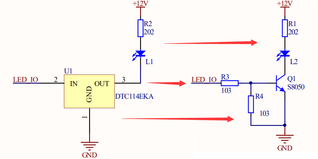

With the development of science and technology, especially the upgrading of electronic technology, the quality requirements of components used in electronic devices are getting higher and higher, and the widespread use of semiconductor devices has degraded their lifespan and eventually led to failure.
A large proportion of electronic components operate in extreme temperatures and harsh environments, causing them to malfunction, and a large number of components are stopped in laboratories and fabs during research and development. Excessive use of humans, surges, and electrostatic breakdowns are the causes of the shortened life of semiconductor devices. In addition, some well-functioning devices are also damaged and component degradation occurs.
The reasons for the failure of semiconductor components are innumerable, mainly in several aspects:
1, the design of components
Chip aging is a growing problem at advanced feature size nodes, but so far most design teams don't have to deal with it. As new reliability requirements are raised in markets such as automobiles, these require a comprehensive analysis of the factors affecting aging, which will undergo major changes.
It is generally known that semiconductor devices age over time, but they are unaware of the aging mechanisms or constraints that lead to chip failure. In addition, there are certain requirements for the shortest life of the device, depending on the application.
It may be 2 or 3 years for consumer devices and up to 10 years for telecom equipment. Given that the aging process is complex and often difficult to fully predict, many chip designs today often employ redundant design methods to ensure sufficient headroom to meet reliable life-long operational requirements.
“In the case of an op amp, it's the basis of a lot of things. The op amp must be properly biased and some margin must be left in the overdrive voltage. Then you have to make sure you leave enough margin so that over time As the op amp ages, it will remain in the saturation region of the transistor. The overdrive margin of the transistor is shrinking because the 7nm supply voltage is 750mV and the threshold is about 350mV, so there is almost no room to retain a large margin. With aging, the threshold voltage can be shifted by up to 50mV. If the op amp bias circuit is offset by 50mV, it may change from a saturated region to a linear region or a triode region, and the transistor will become a resistor without gain. The function is to provide gain, when the circuit becomes useless."
Aging and reliability are challenges for analog designers. Today's designs may not run tomorrow, as these designs may be downgraded, and the most important thing at the moment is to ensure that all aging and reliability requirements of the market are met.
2, the manufacture of components
The fabrication of semiconductor devices involves measuring structures that are only a few nanometers. For reference, the human DNA strand has a diameter of 2.5 nm and the human hair has a diameter of 80,000 to 100,000 nm. A dust can destroy several dies on the wafer.
If the size of the die becomes larger, the probability of random failure increases. For mature process nodes, the yield may be between 80% and 90%. However, for newer nodes, the yield may be well below 50%, although the actual figures are strictly confidential.
“Even if the die is not catastrophically affected, it cannot be considered operational. The manufacturing steps are not perfect, even a process change of an atom can make a significant difference. Although this may not be part of the design. The impact, but if the process changes exactly coincide with the critical timing path, the device may not meet specifications."
As designs evolved into deep sub-micron technology with advanced packaging, existing simulation tools and design methods do not adequately reflect changes and their impact on reliability. This can lead to loopholes in the design process, which can lead to some failures. Design processes are increasingly allowing changes to be considered early in development to minimize their impact, while design techniques such as redundancy can reduce the number of "almost operational" chips that need to be discarded.
3. ESD protection
Typically, the chip will contain ESD protection, and if a voltage of 0.5V is applied to the outside of the chip, an electric field of 0.5 mV/m is produced on a 1 nm medium. This is enough to cause a high voltage arc. For a single die within a package, their goal is a standard of 2kJ.
"If you try to minimize ESD, even eliminate it on these Wide I/O interfaces or any type of multi-chip interface channel, this means you can't really test each chip for your same standard for a single chip. They must be tested more professionally because they have little ESD protection or may not have ESD protection."
ESD events can cause problems even during operation. In portable electronics, ESD can lead to many types of soft errors. During an ESD event, noise may be generated on the power supply network (PDN) due to the sensitivity of some ICs (oscillator ICs, CPUs, and other ICs) or the field coupling of the PDN.
4. The influence of magnetic field on semiconductor
With the multi-functionality of smart phones and tablet terminals, the required power supply voltage also involves various specifications, so the number of inductors used in power supply circuits is increasing. The power supply circuit requires a small size and supports a large current, and requires low loss in some battery-operated devices such as smartphones.
“Inductance stores energy in a magnetic field to perform its function. However, in addition to the electromagnetic energy generated by itself, the inductance is also affected by the external magnetic flux. The inductance value of the component is guaranteed to be the value without the external magnetic flux. Therefore, When the inductor is packaged in the presence of external magnetic flux, it may not be able to perform its intended function."
Therefore, EMS is a new problem that people have to worry about. The energy injection test is to inject 1W of energy from 150kHz up to 1GHz. At each frequency, you will inject 1W of energy into the system. If you don't have enough protection, it will break into the chip's internal circuit along the path, or the voltage on the pin may be too high. If the voltage is too high, it will produce over-stress.
5, switching power supply
Now that the power supply industry has come out of the market downturn in the first three or four years, the competition in the switching power supply market is becoming increasingly fierce. China's power supply companies rely on low-cost manufacturing to have no advantage in the world market. At the same time, foreign power semiconductor supply. The position of the business in the power industry has been further strengthened.
Although the market development situation is optimistic, in the past ten years, Chinese switching power supply companies have relied on low-cost advantages to produce products that meet the requirements of quality and performance parameters of world-renowned OEMs. For success, Chinese power companies have done many links. Investing, more and more semiconductor manufacturers are using embedded power to reduce product costs, and also make power higher and higher.
“The higher the power, the heat of the electronic components, and the problem with heat is not only that the phone gets hot in the pocket. It causes the transistor and the connection between them to degrade, which also directly affects the semiconductor components. Performance and reliability."
The chip runs in a harsh environment and faces great challenges in the life cycle of the product. However, as the manufacturing size becomes smaller and new packaging technologies are adopted, new effects are generated, which directly leads to device performance. The failure of research and development.