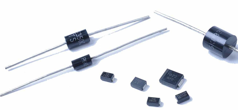

Among the diode electronic components, a device having two electrodes allows current to flow only in a single direction, and many uses the function of rectification. The varactor is used as an electronically tunable capacitor. The current directionality of most diodes is often referred to as the "Rectifying" function. The most common function of a diode is to allow only current to pass in a single direction (called forward bias) and reverse in reverse (called reverse bias).
An early vacuum electronic diode, an electronic device that conducts current in one direction. Inside the semiconductor diode, there is a PN junction and two lead terminals. The electronic device has a unidirectional current conductivity according to the direction of the applied voltage. Generally, a crystal diode is a p-n junction interface formed by sintering a p-type semiconductor and an n-type semiconductor. A space charge layer is formed on both sides of the interface to form a self-built electric field. When the applied voltage is equal to zero, the diffusion current is equal to the drift current caused by the self-built electric field due to the difference in the concentration of carriers on both sides of the p-n junction, and is in an electric equilibrium state, which is also a diode characteristic under normal conditions.
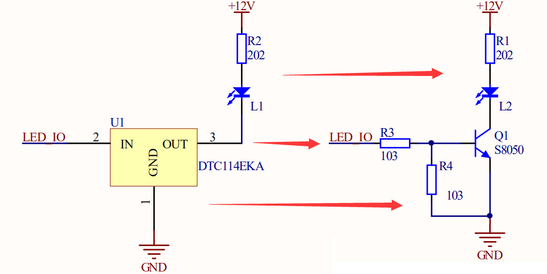
The role of the diode
Diode is one of the most commonly used electronic components. Its biggest characteristic is unidirectional conduction, that is, current can only flow from one direction of the diode. The diode acts as a rectifier circuit (such as 1N4004), detection circuit, and voltage regulator circuit. Various modulation circuits.
How the diode works
The crystal diode is a pn junction formed by a p-type semiconductor and an n-type semiconductor, and a space charge layer is formed on both sides of the interface, and a self-built electric field is built. When there is no applied voltage, the diffusion current caused by the difference in carrier concentration on both sides of the pn junction is equal to the drift current caused by the self-built electric field, and is in an electric equilibrium state. When the outside has a forward voltage bias, the mutual suppression of the external electric field and the self-built electric field causes the diffusion current of the carrier to increase to cause a forward current. When the outside has a reverse voltage bias, the external electric field and the self-built electric field are further strengthened to form a reverse saturation current I0 that is independent of the reverse bias voltage value within a certain reverse voltage range. When the applied reverse voltage is high to a certain extent, the electric field strength in the space charge layer of the pn junction reaches a critical value to generate a multiplication process of carriers, generating a large number of electron hole pairs, and generating a large reverse breakdown current. It is called the breakdown phenomenon of the diode. The reverse breakdown of the pn junction is characterized by Zener breakdown and avalanche breakdown.
In the previous section, we also introduced the identification method of the diode and the test precautions. The main basis is also the working principle of the diode.