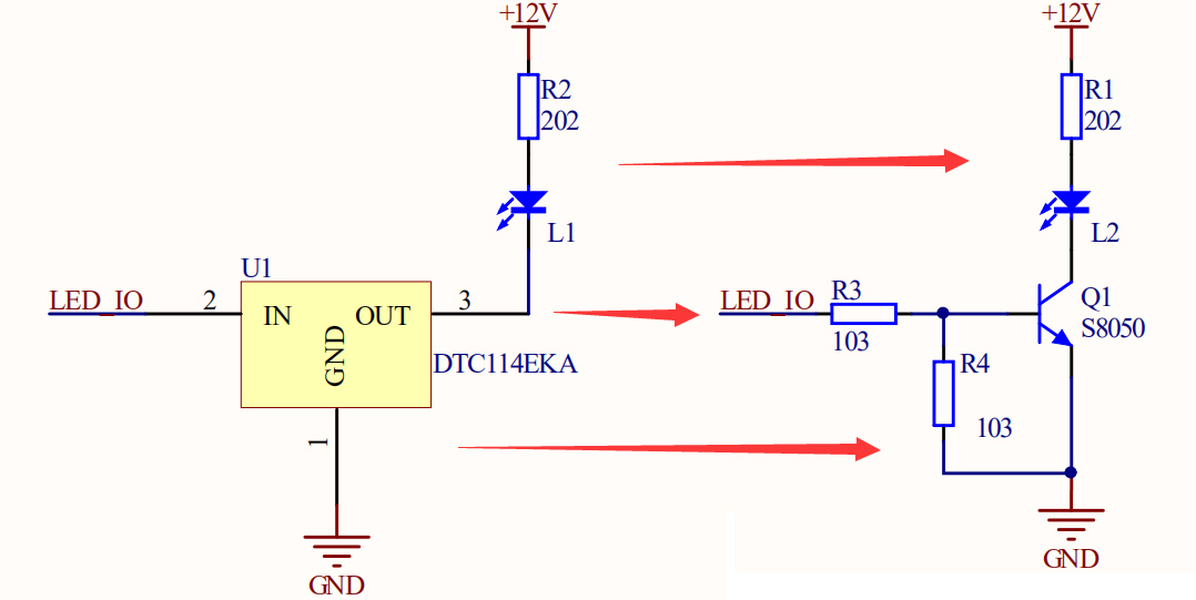

The Schottky diode is a metal-semiconductor device in which a noble metal (gold, silver, aluminum, platinum, etc.) A is a positive electrode, and an N-type semiconductor B is a negative electrode, and a barrier formed on the contact surface thereof has a rectifying property. Since there are a large number of electrons in the N-type semiconductor, and there is only a very small amount of free electrons in the noble metal, the electrons diffuse from the high concentration B to the low concentration A. Obviously, there is no hole in the metal A, and there is no diffusion movement of holes from A to B. As electrons continue to diffuse from B to A, the surface of the B-electron concentration gradually decreases, and the surface electrical neutrality is destroyed, thus forming a potential barrier whose electric field direction is B→A. However, under the action of the electric field, the electrons in A also produce a drift motion from A→B, thereby weakening the electric field formed by the diffusion motion. When a space charge region of a certain width is established, the electron drift caused by the electric field and the electron diffusion motion caused by the difference in concentration reach a relative balance, and a Schottky barrier is formed.
The internal circuit structure of a typical Schottky rectifier is based on an N-type semiconductor on which an N- epitaxial layer using arsenic as a dopant is formed. The anode is made of a material such as molybdenum or aluminum to form a barrier layer. Silica (SiO2) is used to eliminate the electric field in the edge region and increase the withstand voltage of the tube. The N-type substrate has a small on-state resistance, and its doping concentration is 100% higher than that of the H-layer. An N+ cathode layer is formed under the substrate to reduce the contact resistance of the cathode. By adjusting the structural parameters, a Schottky barrier is formed between the N-type substrate and the anode metal as shown. When a forward bias is applied to both ends of the Schottky barrier (anode metal is connected to the positive electrode of the power supply, and the N-type substrate is connected to the negative electrode of the power supply), the Schottky barrier layer is narrowed, and the internal resistance becomes small; When a reverse bias is applied across the Schottky barrier, the Schottky barrier layer becomes wider and its internal resistance becomes larger.
In summary, the structural principle of the Schottky rectifier is very different from that of the PN junction rectifier. The PN junction rectifier is usually called a junction rectifier, and the metal-semiconductor rectifier is called a Schottky rectifier. In recent years, aluminum-silicon Schottky diodes fabricated using a silicon planar process have also been introduced, which not only saves precious metals, significantly reduces costs, but also improves parameter consistency. A comparison of Schottky diode characteristic curves can be seen.
Due to its robust structure, fast response and low clutter, Schottky diodes are widely used in high frequency circuits. In recent years, it has also been used in low-voltage, high-current power circuits and AC-DC converter systems.