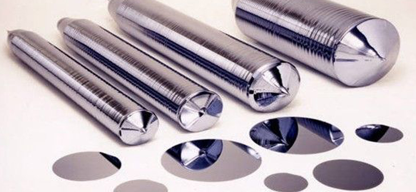

semiconductor
The material is taken from the junction of metals and nonmetals in the periodic table. The conductivity of the semiconductor at room temperature is between the conductor and the insulator.
Intrinsic semiconductor
A pure semiconductor with a crystal structure is called an intrinsic semiconductor. (Because it contains no impurities and is crystal structure, its conductivity is worse than that of ordinary semiconductors)
At room temperature, a small number of valence electrons get enough energy due to thermal motion to break free from the bond of covalent bonds. At this point, the covalent bond leaves an empty position, ie a hole. An atom is positively charged by the loss of electrons, or the hole is positively charged. An electric field is applied to the intrinsic semiconductor, and the free electrons will move in a direction to generate a current. At the same time, the valence electrons will fill the holes in a certain direction, which is equivalent to the directional movement of the holes, and the movement opposite to the electrons. The current of the intrinsic semiconductor is the sum of these two currents. The particles carrying the charge are called carriers.
When there is a free electron, there is bound to be a hole, so the free electron and the hole pair are the same. When free electrons fill a hole in motion, both of them disappear at the same time. This phenomenon is called compounding. At a certain temperature, the two carrier concentrations are the same, achieving a dynamic equilibrium. When the temperature rises, the thermal motion will intensify, and more electrons will break free from binding, which will cause the carrier concentration to rise, thus breaking the balance, and the equilibrium will be established again after the temperature is constant.
Impurity semiconductor
Some elements are incorporated in the intrinsic semiconductor by a diffusion process.
An N-type semiconductor
The addition of +5-valent elemental phosphorus to the intrinsic semiconductor, due to the addition of the five elements of the outermost layer, will produce an additional electron after the formation of the covalent bond, and this electron becomes a free electron. Since the number of free electrons in this semiconductor is more than the number of holes, and the electrons are negatively charged, they are called N (negative) semiconductors.
2. P-type semiconductor
Adding +3 valent element boron to the intrinsic semiconductor, because the element with the outermost layer of 3 electrons is added, a vacancy will be formed after the formation of the covalent bond, and the outermost electron of the silicon atom will fill the vacancy. There will be more holes. The hole is positively charged, so it is called a P (positive) type semiconductor.
In an N-type semiconductor, a free electron is a majority carrier, and a hole is a minority carrier; in a P-type semiconductor, a hole is a majority carrier, and a free electron is a minority carrier.
Formation of PN junction
A P-type semiconductor and an N-type semiconductor can be fabricated on the same silicon wafer by a certain process.
Due to the difference in concentration, a diffusion motion occurs. At the same time, at the junction of the N region of the P region, the majority of the carrier concentration decreases, the positive ion region appears in the P region, and the negative ion region appears in the N region, and an internal electric field is generated inside. This electric field produces a motion to prevent the diffusion motion, which is called drift motion. The number of carriers participating in the diffusion motion and the drift motion is the same, and the dynamic balance forms a PN junction.
Capacitance effect of PN junction
The PN junction has an equivalent capacitance (barrier capacitance and diffusion capacitance, the sum of the two is called junction capacitance, specifically omitted). Since the capacitive reactance is inversely proportional to the frequency, when the frequency of the alternating current applied to the PN junction is high, the alternating current It is possible to form a via through the capacitance of the PN junction, and the PN junction loses the characteristic of unidirectional conduction.


