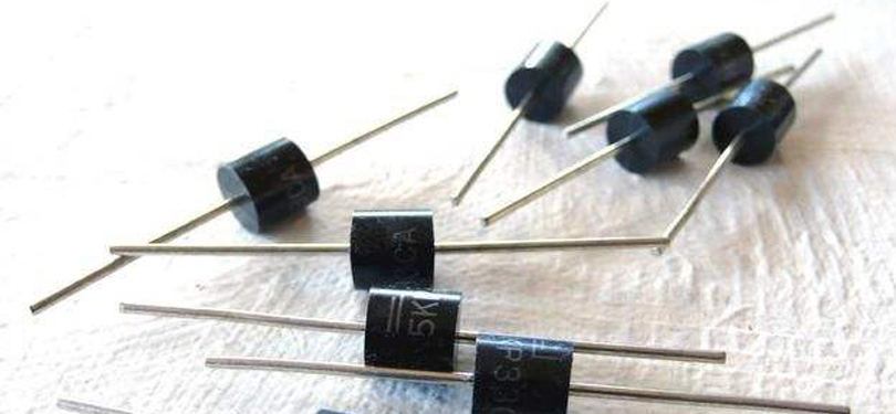

First, classified by semiconductor materials
Diodes can be classified into germanium (Ge) diodes, silicon (Si) diodes, gallium arsenide (GaAs) diodes, gallium phosphide (GaP) diodes, and the like according to the materials used.
Second, classified by package form
Diodes are classified into plastic diodes, glass diodes, metal diodes, chip diodes, and leadless cylindrical diodes in their package.
Third, by structure
Semiconductor diodes mainly rely on PN junctions to work. The point contact type and Schottky type which are inseparable from the PN junction are also included in the range of general diodes. Including these two models, according to the characteristics of the PN structure, the crystal diodes are classified as follows:
1, point contact diode
The point contact type diode is formed by pressing a metal pin on a single wafer of germanium or silicon material and then performing an electric current method. Therefore, the PN junction has a small electrostatic capacitance and is suitable for use in a high frequency circuit. However, compared with the junction type, the point contact type diode has poor forward characteristics and reverse characteristics, and therefore cannot be used for large current and rectification. Because of its simple construction, it is cheap. It is a widely used type for general purposes such as detection, rectification, modulation, mixing and limiting of small signals.
2, key diode
The key diode is formed by fusing or silver filaments on a single wafer of germanium or silicon. Its characteristics are between the point contact diode and the alloy diode. Compared with the point contact type, although the PN junction capacitance of the key diode is slightly increased, the forward characteristic is particularly excellent. It is used for switching, and is sometimes used for detection and power rectification (not more than 50mA). In a key diode, a diode that fuses a gold wire is sometimes referred to as a gold bond type, and a diode that fuses a silver wire is sometimes referred to as a silver bond type.
3. Alloy diode
A PN junction is formed by a method of alloying a metal such as indium or aluminum on a single wafer of N-type germanium or silicon. The forward voltage drop is small, suitable for high current rectification. Since the PN junction is reversed with a large capacitance, it is not suitable for high frequency detection and high frequency rectification.
4, diffusion diode
In a high-temperature P-type impurity gas, a single wafer of N-type germanium or silicon is heated to make a portion of the surface of the single wafer P-type, and the PN junction is obtained by this method. Due to the small forward voltage drop of the PN junction, it is suitable for high current rectification. Recently, the mainstream of using large current rectifiers has been transferred from a silicon alloy type to a silicon diffusion type.
5, mesa type diode
Although the PN junction is fabricated in the same manner as the diffusion type, only the PN junction and its necessary portions are retained, and unnecessary portions are corroded with chemicals. The rest of the section is in the shape of a countertop, hence the name. The countertop type that was initially produced was made by using a diffusion method for semiconductor materials. Therefore, this type of mesa is called a diffusion mesa. For this type, it seems that there are few models for high current rectification, and there are many models for small current switches.
6, planar diode
On a semiconductor single wafer (mainly an N-type silicon single wafer), a P-type impurity is diffused, and a PN junction formed by selectively diffusing only a part of the N-type silicon single crystal wafer is utilized by the shielding action of the surface oxide film of the silicon wafer. Therefore, there is no need for the corrosive action of the drug for adjusting the PN junction area. The semiconductor surface is named because it is made flat. Further, since the surface of the PN bond is covered by the oxide film, it is recognized as a type having good stability and long life. Initially, the semiconductor material used was formed by an epitaxial method, and the planar type was also referred to as an epitaxial planar type. For planar diodes, it seems that there are few models for high current rectification, and there are many models for small current switches.
7, alloy diffusion diode
It is a type of alloy. Alloy materials are materials that are easily diffused. By making the difficult-to-manufacture material by subtly blending the impurities, it is possible to over-dif with the alloy to obtain an appropriate concentration distribution of the impurities in the already formed PN junction. This method is suitable for manufacturing high sensitivity varactor diodes.
8, epitaxial diode
A diode formed by fabricating a PN junction by a process of epitaxial length. Very high technology is required for manufacturing. Since it is possible to arbitrarily control the distribution of different concentrations of impurities, it is suitable for manufacturing a highly sensitive varactor.
9, Schottky diode
The basic principle is to block the reverse voltage with the already formed Schottky on the contact surface of the metal (for example, lead) and the semiconductor (N-type silicon wafer). There is a fundamental difference between the Schottky and PN junction rectification principles. Its pressure resistance is only about 40V. Its speciality is: the switching speed is very fast: the reverse recovery time trr is particularly short. Therefore, a switching diode and a low-voltage high-current rectifier diode can be fabricated.


